Beyond Moore's Law: New Memory Chip Defies Miniaturization Limits, Promises Ultra-Efficient Electronics
Scientists have engineered a groundbreaking memory chip that challenges long-held principles of miniaturization, potentially revolutionizing electronics. This new device not only shrinks components to an extreme scale but also reduces energy loss as it gets smaller, addressing critical issues like overheating and battery drain. This innovation could lead to a new generation of ultra-efficient smartphones, wearables, and advanced AI systems, marking a significant leap in computing technology.
For decades, the relentless march of technological progress has been dictated by Moore's Law, the observation that the number of transistors on a microchip doubles approximately every two years. This principle has driven the exponential growth in computing power, making our devices faster, smaller, and more capable. However, this progress has come with an increasingly challenging trade-off: as components shrink, they tend to generate more heat and consume more power, leading to issues like overheating, reduced battery life, and significant energy demands for data centers. Now, a team of pioneering scientists has unveiled a memory chip that not only breaks free from these constraints but actually improves in efficiency as it gets smaller, a feat once considered impossible.
This groundbreaking development could finally solve the perennial problem of energy inefficiency in modern electronics, paving the way for a new era of ultra-efficient devices, from smartphones and wearables to advanced artificial intelligence systems. The implications are profound, promising not just longer battery life but also a significant reduction in the environmental footprint of digital technology.
The Miniaturization Paradox: A Looming Crisis
The fundamental challenge in modern electronics lies in the physics of miniaturization. As transistors and memory cells shrink to atomic scales, the electrical resistance within them tends to increase, leading to greater energy dissipation in the form of heat. This phenomenon, often referred to as the "power wall," has been a major hurdle for engineers. Traditional memory devices store information by controlling the ease with which electricity passes through a material, representing binary 0s and 1s. To achieve higher densities and speeds, these components have been packed ever more tightly, exacerbating the heat and power consumption problem. Data centers, for instance, consume vast amounts of electricity, much of it dedicated to cooling the thousands of servers that generate immense heat. For portable devices, this translates directly into shorter battery life and the need for larger, heavier batteries.
Experts have long warned that without a fundamental shift in material science and device architecture, the benefits of miniaturization would soon be outweighed by its energetic costs. "We've been pushing the limits of silicon for so long, and while we've found clever ways to mitigate some of these issues, the underlying physics remains," explains Dr. Anya Sharma, a leading materials scientist specializing in nanotechnology. "To truly break through, we needed something radically different, something that fundamentally rethinks how memory stores and processes information at the atomic level."
Redefining Memory: A New Paradigm
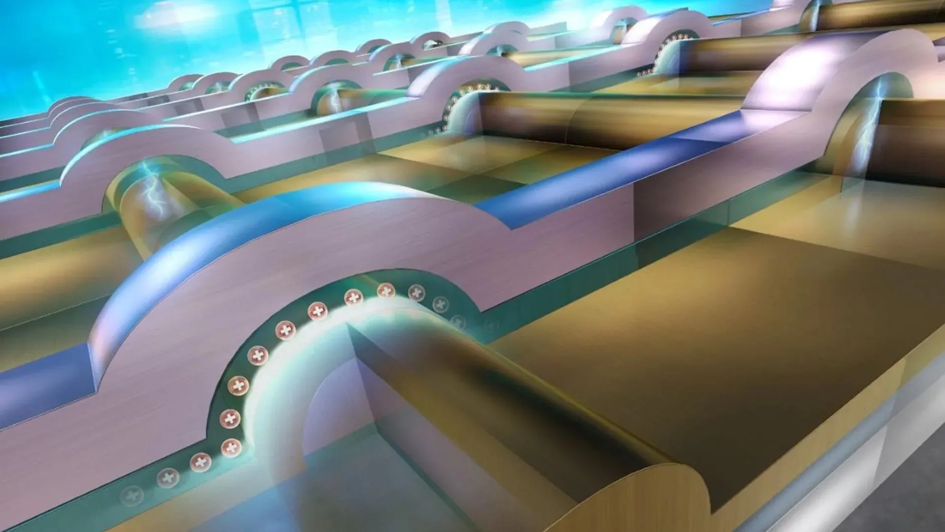
The breakthrough lies in a novel design that reconfigures the very structure of memory components at an extreme scale. Instead of simply making existing designs smaller, the researchers developed a new kind of memory unit that, counter-intuitively, becomes more energy-efficient as its dimensions are reduced. This defies the conventional wisdom that smaller components inherently mean higher energy density and heat generation. The specifics of the material science involved are complex, but at its core, the innovation involves manipulating quantum mechanical properties to control electron flow with unprecedented precision and minimal resistance.
One of the key aspects of this new memory device is its ability to reduce energy loss rather than increasing it. This is achieved through a combination of novel materials and an architectural design that minimizes parasitic resistances and leakage currents, which are major culprits in energy waste in conventional chips. By optimizing the pathways for electrical signals, the scientists have managed to create a system where the energy required to switch a memory state (from 0 to 1 or vice-versa) decreases with scale, rather than increasing. This is a monumental shift from previous approaches.
Implications for a Connected World
The potential impact of this technology is immense and far-reaching:
* Smartphones and Wearables: Imagine a smartphone that lasts for days on a single charge, or a smartwatch that can perform complex tasks without needing daily recharging. This new memory could dramatically extend battery life, making portable electronics truly ubiquitous and always-on. * Artificial Intelligence and Machine Learning: AI systems, particularly those involving deep learning, are notoriously power-hungry. Training large neural networks requires immense computational resources and energy. More efficient memory would allow for the development of more powerful, yet energy-frugal, AI accelerators, enabling advanced AI to run on edge devices without relying solely on cloud computing. * Data Centers: Reducing the energy consumption of memory in servers would have a cascading effect. Lower power draw means less heat, which in turn means less energy spent on cooling. This could lead to significantly greener data centers, reducing operational costs and environmental impact. * Internet of Things (IoT): The proliferation of IoT devices, from smart sensors to connected appliances, demands low-power components that can operate autonomously for extended periods. This new memory could be a game-changer for enabling truly pervasive and sustainable IoT ecosystems. * Edge Computing: With more processing power and memory available at the "edge" of the network (i.e., closer to the data source), devices can perform more tasks locally, reducing latency and reliance on centralized cloud resources. This is crucial for applications like autonomous vehicles and real-time industrial automation.
This breakthrough is not merely an incremental improvement; it represents a fundamental rethinking of how memory operates. It suggests that the path to continued technological advancement might not be solely about pushing existing paradigms to their limits, but about discovering entirely new ones. The ability for a component to become more efficient as it shrinks is a profound reversal of established engineering challenges.
The Road Ahead: From Lab to Market
While the initial results are incredibly promising, the journey from laboratory prototype to mass-market adoption is often long and complex. Researchers will need to demonstrate scalability, reliability, and cost-effectiveness in manufacturing. Integrating this new memory architecture into existing semiconductor fabrication processes will be a significant engineering challenge. However, the potential rewards are so substantial that investment and research are likely to accelerate rapidly.
This development signals a hopeful future where our digital lives can continue to expand without being constrained by the physical limitations of energy consumption and heat dissipation. It suggests that the next generation of electronics will not only be faster and more powerful but also inherently more sustainable. As we stand on the cusp of an era where computing is embedded in every aspect of our lives, from smart cities to personalized healthcare, the ability to build devices that are both potent and parsimonious with energy will be paramount. This new memory chip is not just a scientific curiosity; it's a blueprint for a more efficient, sustainable, and powerful technological future, truly breaking the rules of miniaturization and opening up a world of possibilities that were once deemed impossible.
Stay Informed
Get the world's most important stories delivered to your inbox.
No spam, unsubscribe anytime.
Comments
No comments yet. Be the first to share your thoughts!